Information to Atoms
How Google DeepMind's AlphaEvolve improved the speed of Substrate's computational lithography stack by 680% and reduced compute costs by 97%, enabling the simulation and printing of the most demanding layers in advanced semiconductor devices.
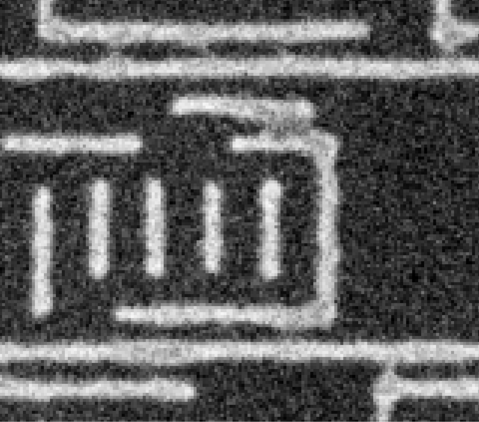
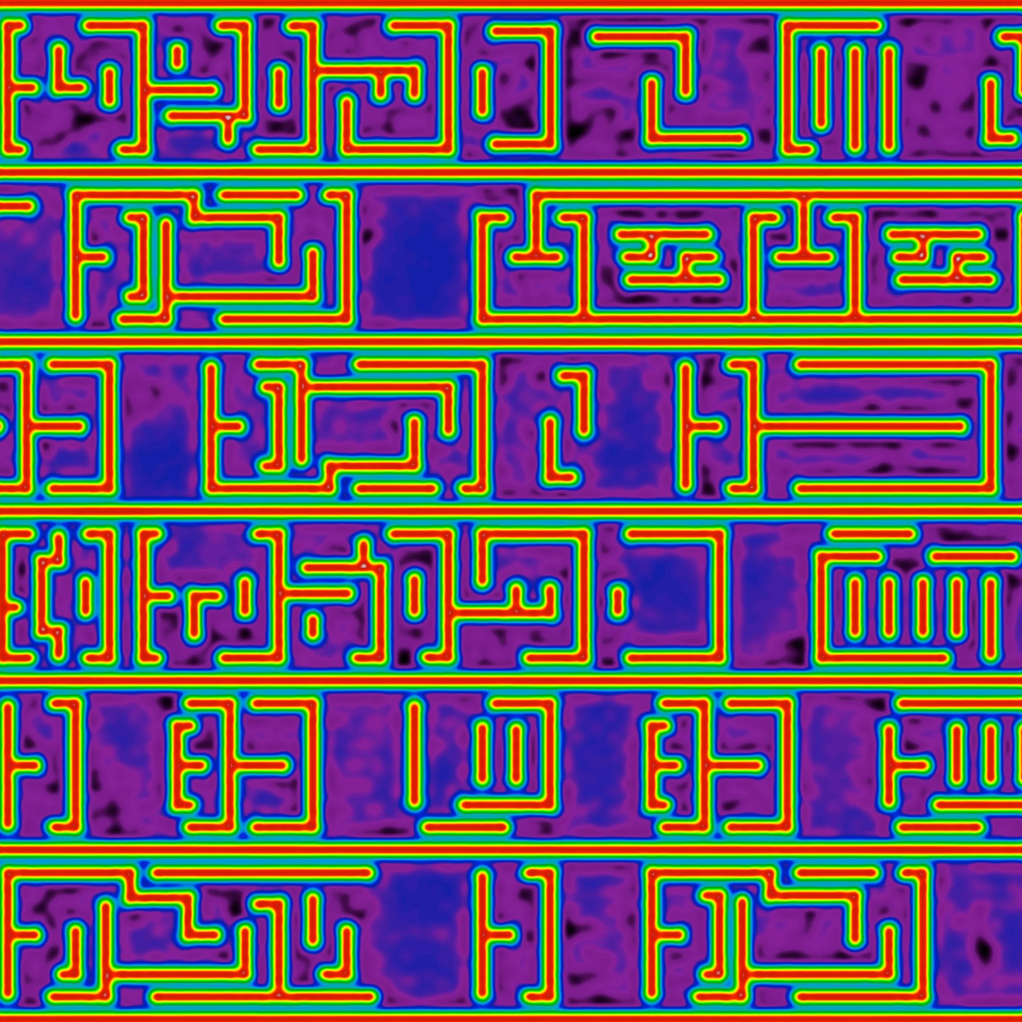 Simulated P24 M1 pattern
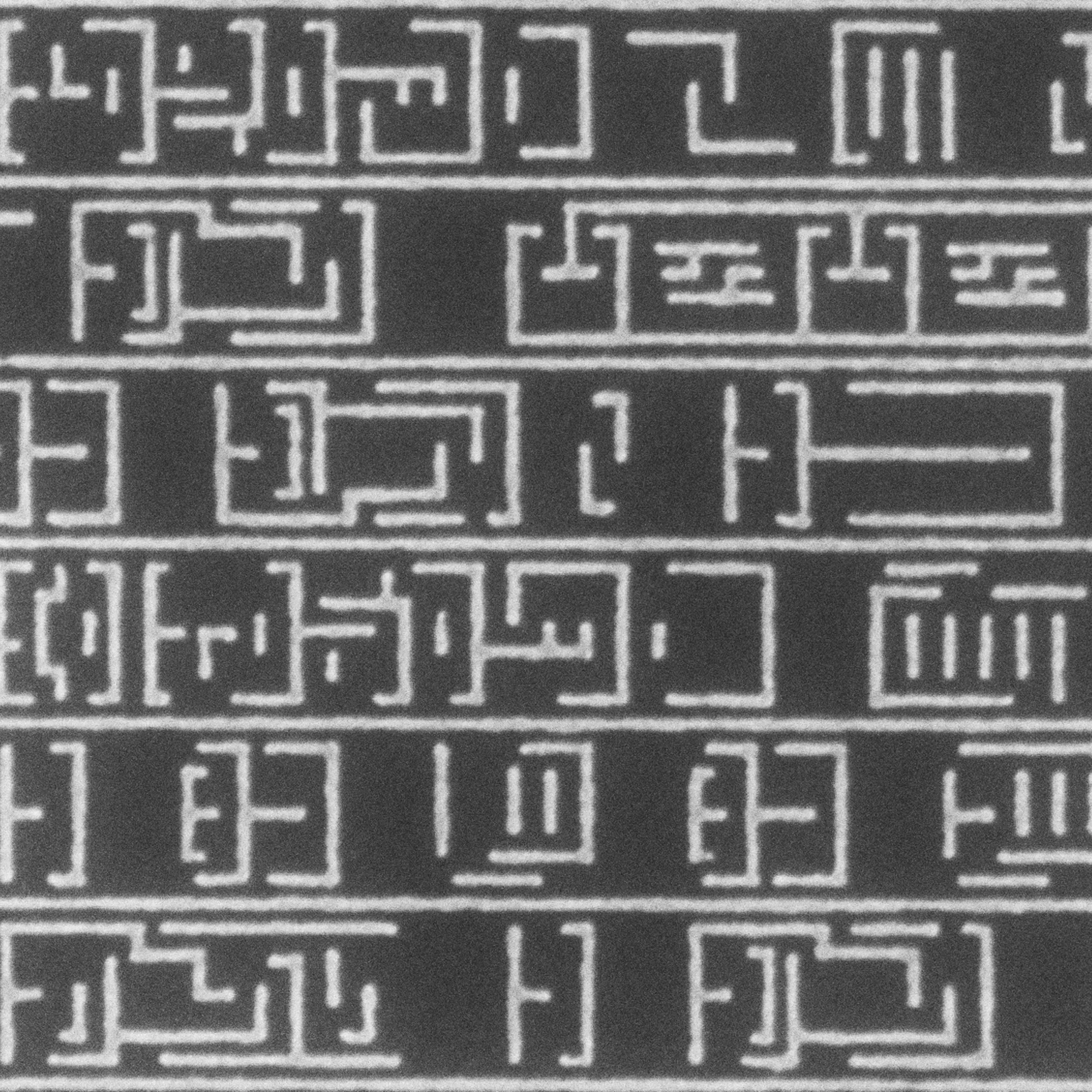 Printed P24 M1 (12 nm CD) with Substrate's X-ray lithography
Over the past several months, AI models fueled by the growing compute infrastructure that powers them have advanced at an incredible pace. This virtuous cycle of model progress driven by greater computing power continues to accelerate, with fabless semiconductor companies now incorporating AI models into their design processes, directly enabling future model improvement cycles.
One of Substrate's founding convictions is that we would reach a point where AI models and the chips that power them would co-evolve—both building each other to compound improvements and shorten time-to-market. By extending this co-design process all the way down to the fabrication of semiconductors themselves, we allow AI to build itself at the atomic level, offering access to intelligence limited only by physics.
The recent addition of Google DeepMind's AlphaEvolve, a Gemini-powered coding agent for designing advanced algorithms, to our work has given us an even clearer idea of how rapid this model-to-fabrication iteration loop will be.
Lithography is the science of information transfer
When printing patterns mere tens of atoms wide, anything and everything can affect the accuracy of information transfer from the mask to the wafer. Even the vibrations from nearby footsteps are enough to blur patterns, and at X-ray wavelengths, air itself will absorb these photons. To ensure the patterning fidelity that advanced semiconductors need, you must master all of the physics governing the lithographic process.
To achieve this, we built a powerful computational lithography stack that includes processes like inverse lithography technology (ILT)1, which works backward from desired patterns to design optimal masks, and optical proximity correction (OPC)2, which adjusts mask designs to correct for distortions during printing. Our end-to-end framework co-optimizes these and other factors into our optics, masks, and patterns to ensure we print the highest-quality, highest-resolution structures possible.
Using X-ray lithography to produce the smallest, most intricate structures humans have ever made requires simulating the paths of many trillions of photons as they bounce across optics, masks, and their interactions with the thin layer of light-sensitive photoresist on a silicon wafer. This level of simulation is extraordinarily computationally intensive.
Traditionally, CPU solvers would take days to weeks, prohibiting their use for achieving realistic end-to-end physics fidelity and making it difficult to model a process with near certainty. We design everything Substrate builds for accelerated computation from day one; without leveraging the very latest computational power, our work would not be possible. And, as with any large computational task, we relentlessly optimize scalability, cost, and runtime.
To give a sense of scale, at 1 nanometer (nm) resolution, a simulation of a printed layer of a full-sized semiconductor die would be hundreds of terapixels (a terapixel is a million million pixels). In reality, we are forced to simulate smaller, but still representative, areas. Even then, the tensor operations involved are enormous, and quickly become a complex, distributed, accelerated-computing problem.
Discovering algorithmic leaps with AlphaEvolve
Over a couple of months, we worked closely with the Google team to integrate AlphaEvolve into our efforts and apply it to some of our most important challenges, including optimizing our computational lithography framework. Initially accelerated by GPUs and now also by TPUs, we have built an end-to-end, differentiable, and scalable simulation stack that handles the most complex physics ever used in semiconductor production.
Below are simulations and printed-on-silicon images from a scanning electron microscope (SEM) of a complex metal one (M1) layer printed in a single exposure with Substrate's X-ray lithography tool, enabled by AlphaEvolve-optimized simulations. The printed patterns are equivalent in resolution to "high numerical aperture" (High-NA) lithography, which is equivalent to the requirements of the 2 nm semiconductor node.
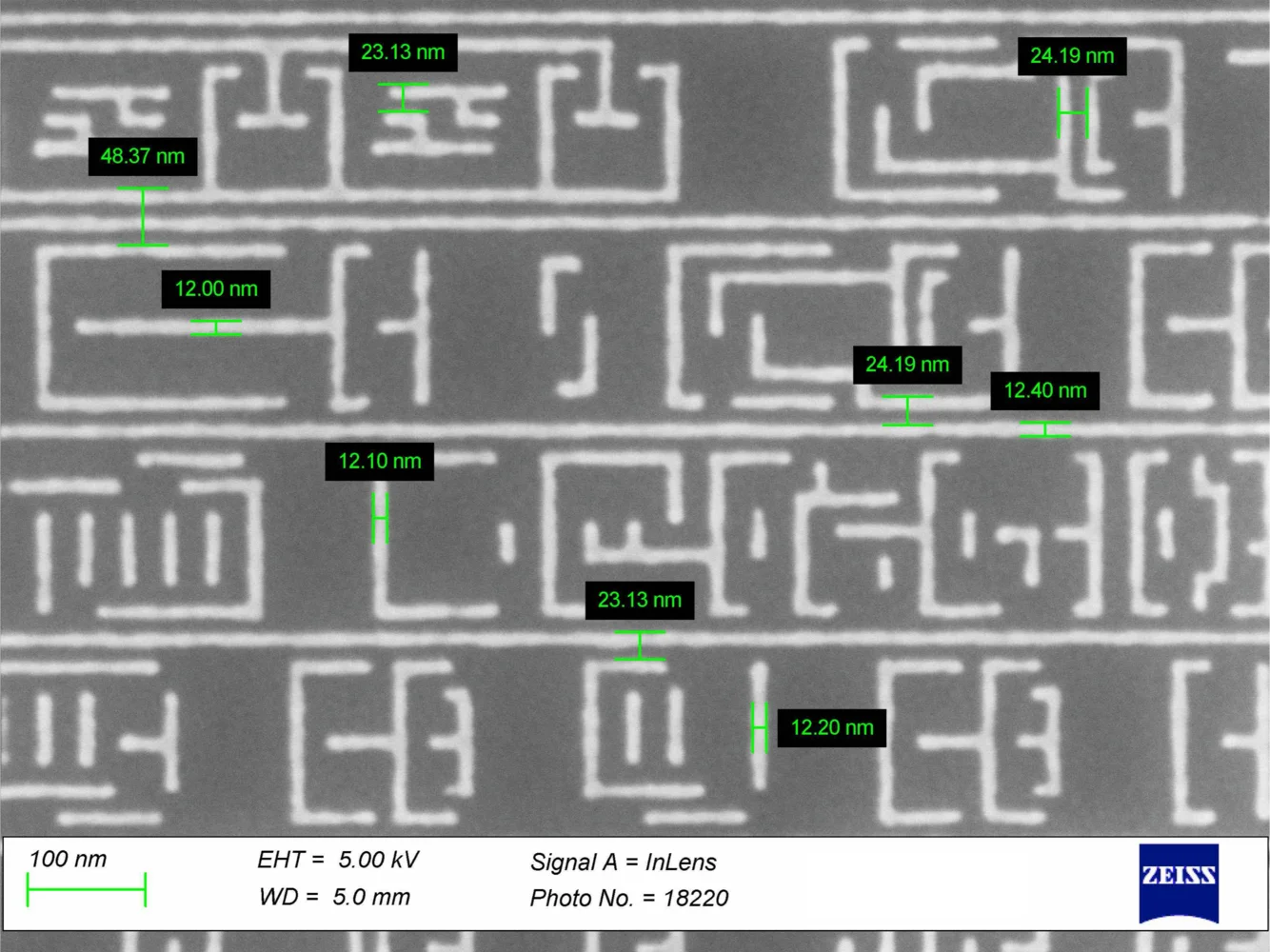 Printed P24 M1 pattern with measurements
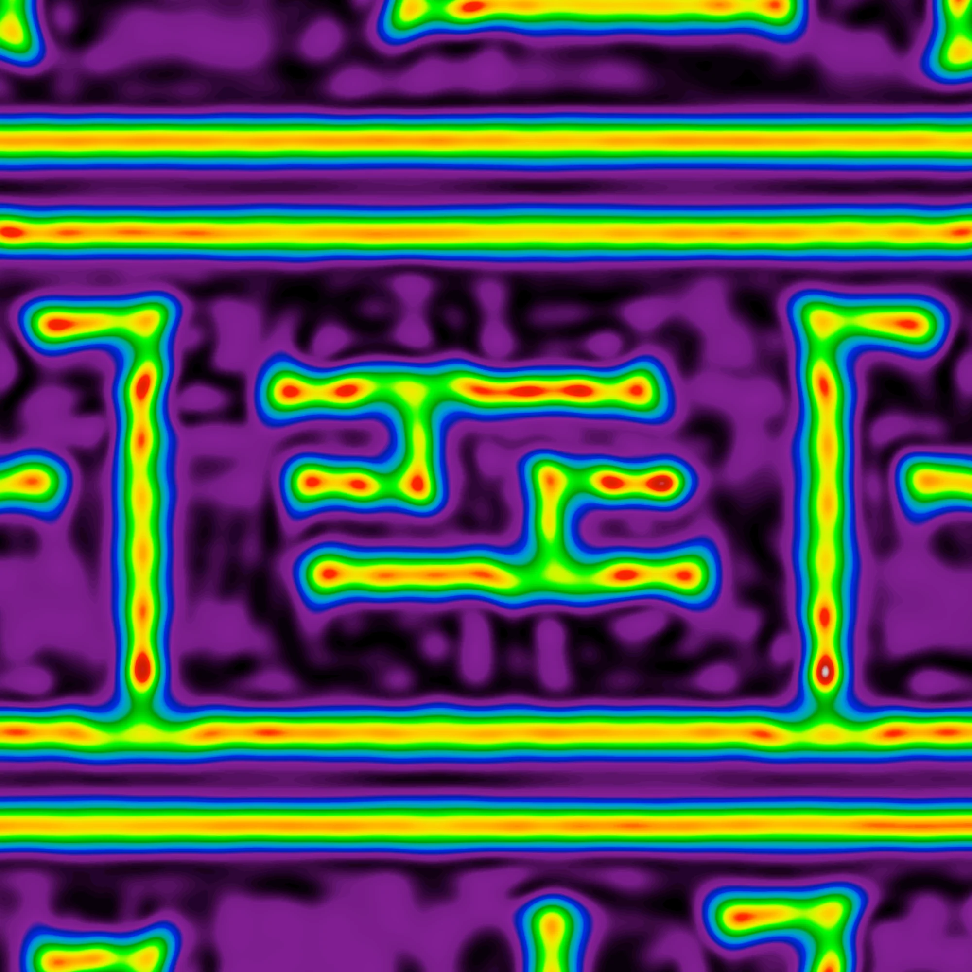 Simulated P24 (12 nm CD) claw pattern
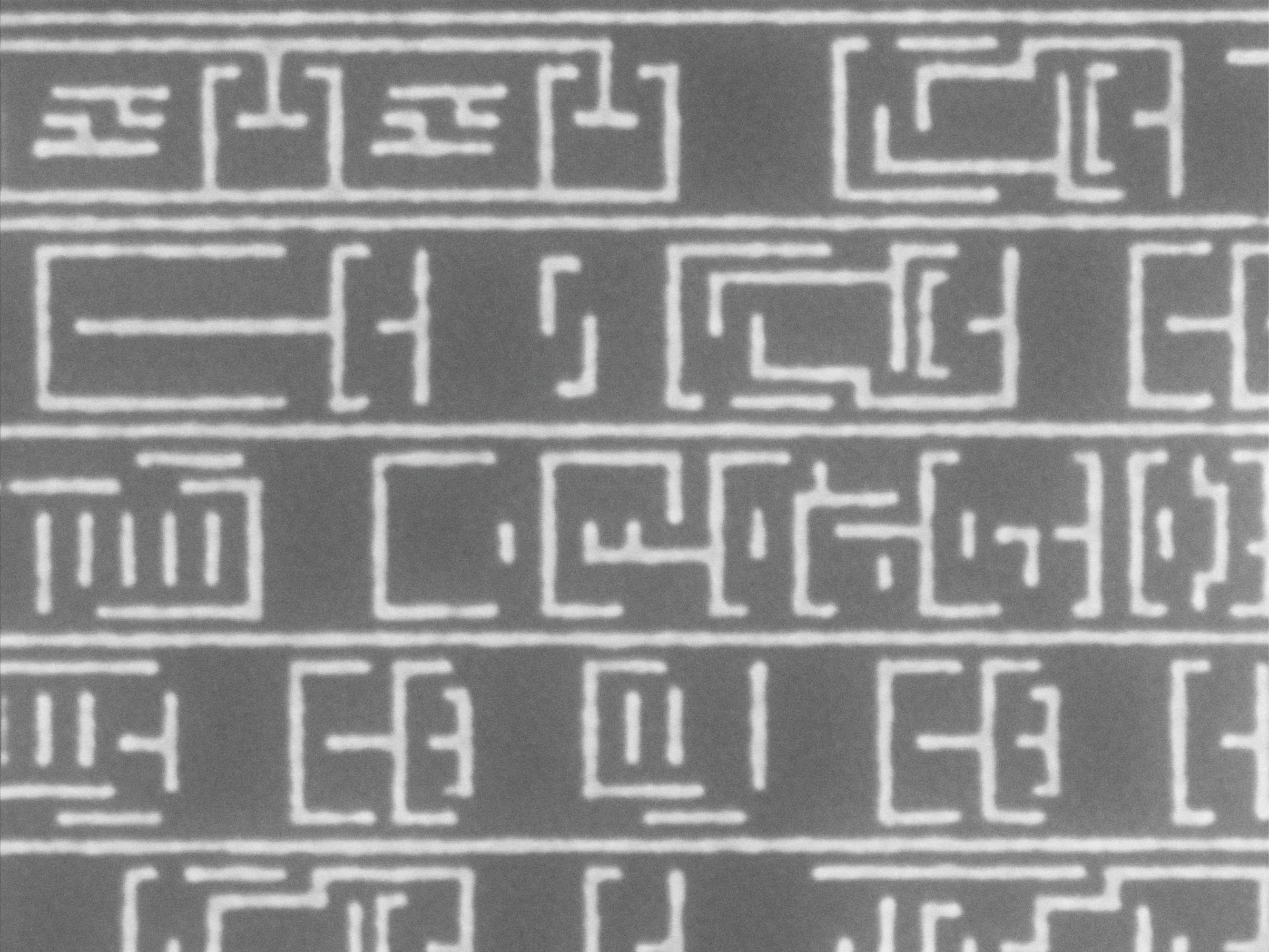 Printed P24 M1 pattern
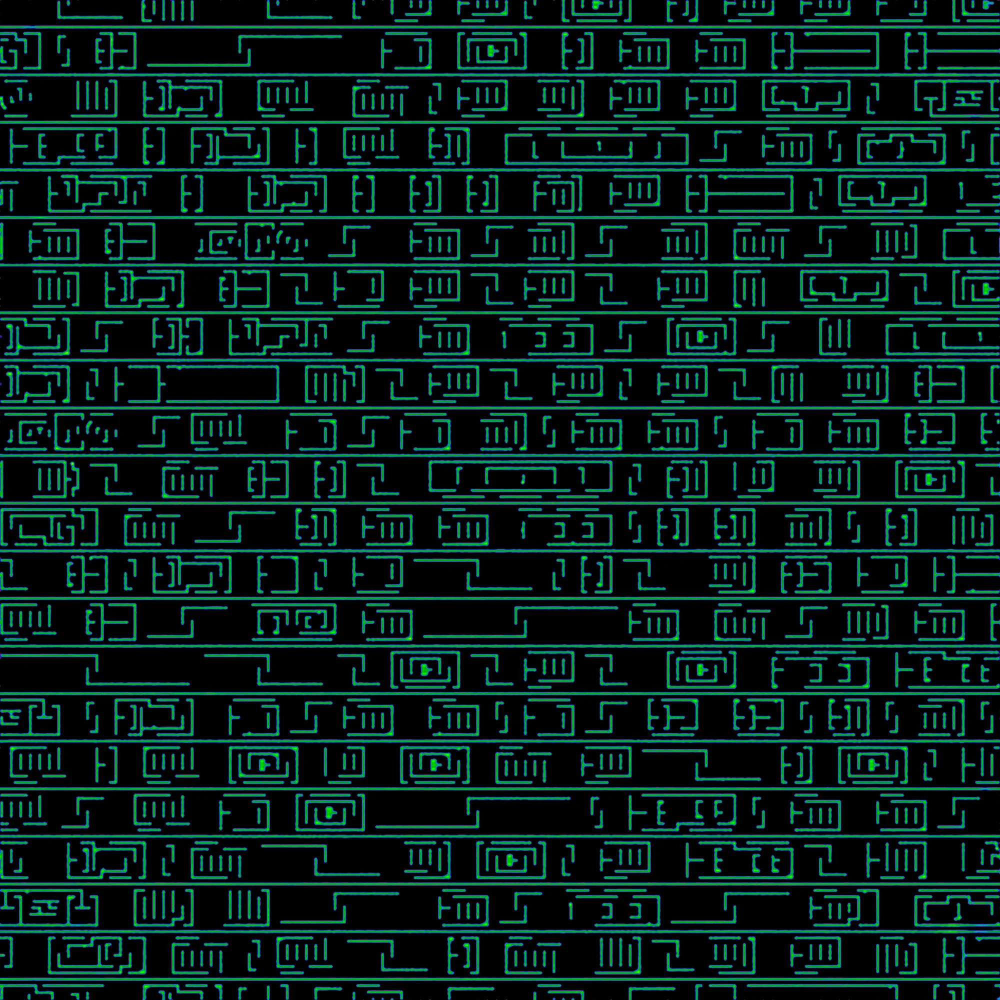 Simulated dose study
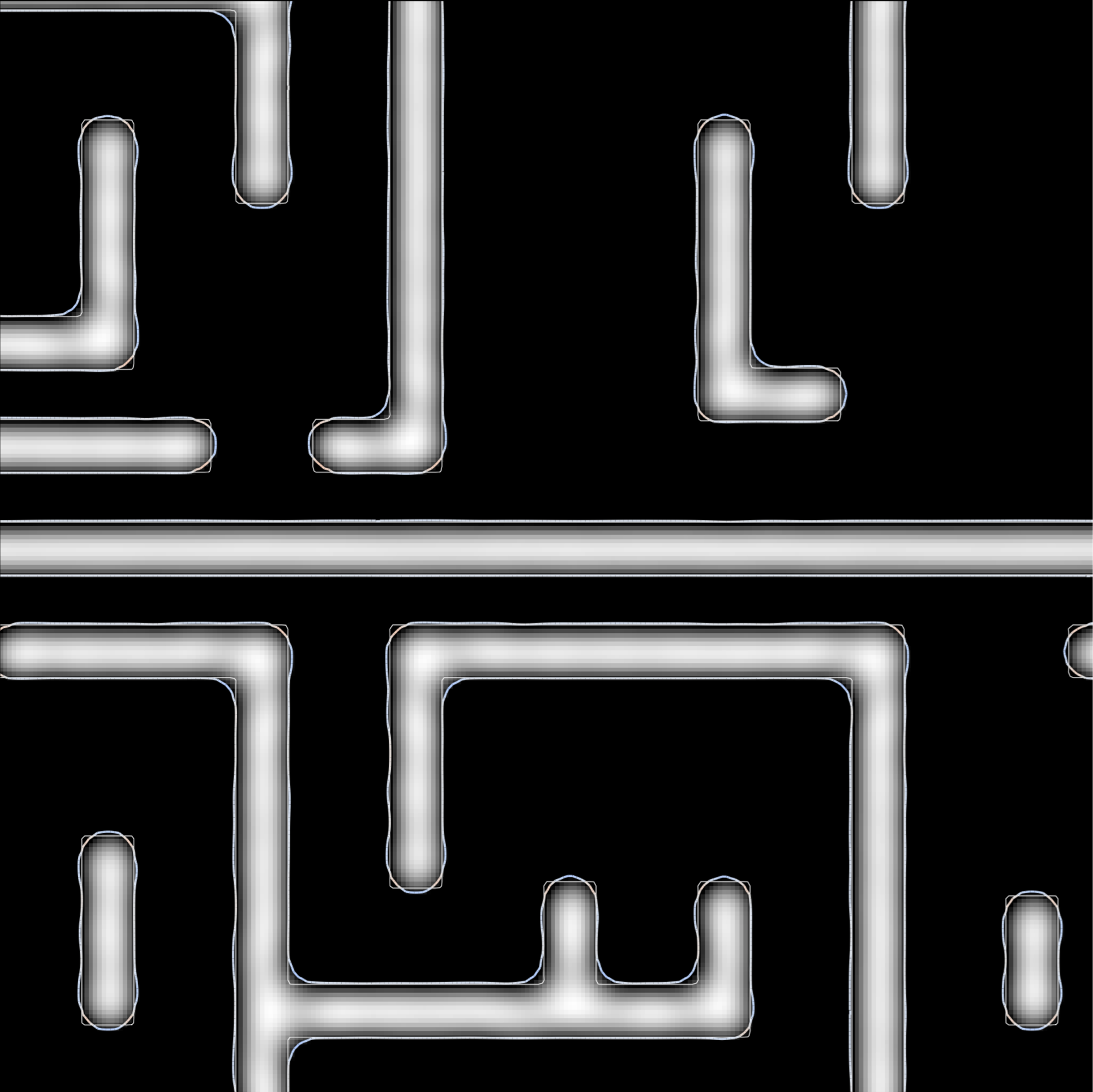 OPC pattern
The M1 layer is the most complex layer of a chip, as it contains routing to connect the transistors below and local interconnects for standard cells, making it by far the most demanding lithographic layer to print. As the sharp 90-degree corners and arbitrary 2D shapes at a 24 nm pitch3 (12 nm half-pitch) demonstrate, Substrate's X-ray lithography tool prints the most demanding layers in a process, all with a single mask and single exposure.
 Triple patterning (3 exposures)

Current advanced semiconductor process nodes require multi-patterning4, a process where a single layer is exposed or processed multiple times to achieve finer feature pitches beyond the resolution of a lithography system.
Template-based approaches work by defining an initial pattern and then using deposition and etching to multiply the number of lines, but because this process produces only parallel lines, it often restricts signal routing to a single direction (1D) per metal layer. This drives the need for more metal layers and connections (vias) between them, introducing higher resistive-capacitive delay and power consumption per computation. Each extra layer increases the total number of processing steps, raising defect risk, extending production time, and increasing wafer cost.
We printed bidirectional (2D) M1 layers with a single, high-power X-ray exposure. Fewer process steps mean faster production, lower-cost wafers, and chips with lower power use and improved performance.
Failing fast to defeat defects
Beyond optimizing for success, the real power of this framework is its ability to predict not just that something will fail, but why. When we understand where and why printing fidelity breaks down, we can compensate by adjusting other parameters, simulate, and then validate with real-world printing.
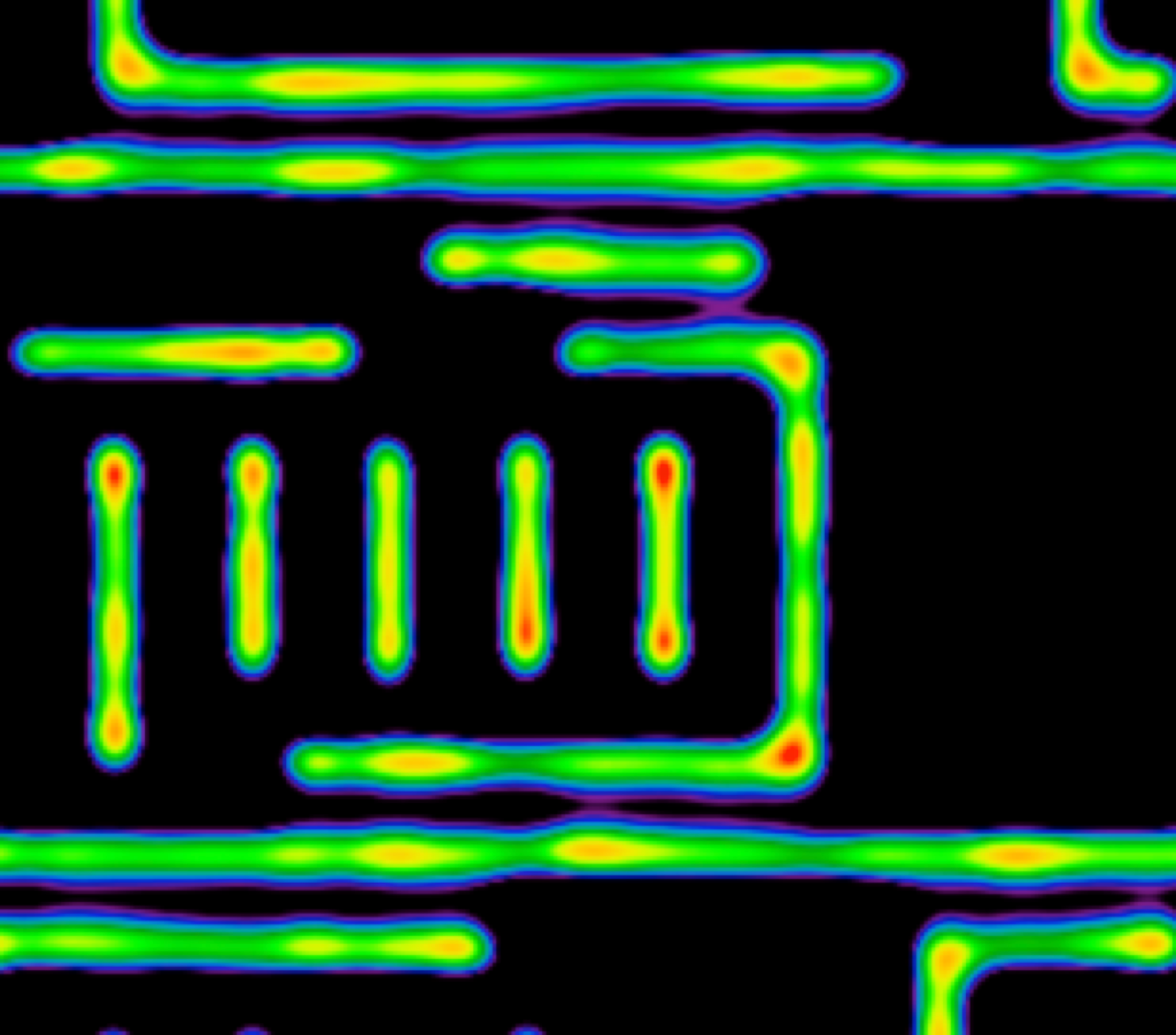
 PrintedSimulated
Bridging defect (left) overlaid with simulation (right) showing increased photon field in purple, which predicts likely bridging
With this predictive capability, we can solve issues with our process before ever reaching the silicon. When you extrapolate across how many wafers are usually run for equivalent changes, you can compress timelines in ways previously not possible. For example, we have achieved printing complex, bidirectional (2D) M1 patterns at P24 (12 nm CD) in many orders of magnitude fewer wafer starts when compared to other leading-edge lithography tools.
The magic of AlphaEvolve
AlphaEvolve has enabled our team to automate the exploration of hundreds of thousands of potential improvements to our algorithms, something that was previously impossible. The magic lies in AlphaEvolve's ability to leverage Gemini's coding models to generate algorithmic hypotheses, mutate code, and autonomously test them, enabling rapid discovery of algorithmic improvements and performance gains.
To our surprise, AlphaEvolve discovered a form of lossless compression that downsampled high-resolution calculations to much lower resolutions than we previously thought possible, without breaking the underlying physics. AlphaEvolve's strength lies in its automatic validation of every experiment through its evaluator framework, which scores results against ground-truth samples and gives confidence in even unintuitive algorithmic pathways.
Enabled by this lossless compression, AlphaEvolve flawlessly identified opportunities in our code to switch to lower-precision numerical representations while preserving the fidelity of our physics operations with little to no information loss in the final simulated results.
A byproduct of these discoveries in compression and numerical precision was that optimizations previously not suitable for running on Google Cloud TPUs suddenly became a perfect match, leading to further incremental speed-ups and cost reductions.
After only one week with AlphaEvolve, we halved our compute costs. After a month of AlphaEvolve co-designing algorithms with our team, our compute costs for the same optimization were reduced by 97%, our equivalent memory usage was 74% lower, and runtime speed was improved by 680%.
By combining countless discoveries in this short time, AlphaEvolve reduced the computational burden of previously prohibitively intensive simulations by orders of magnitude, allowing us to run significantly larger simulations with far less compute. We are now running many more simulations than before, not fewer.
Ultimately, faster and more scalable simulation translates directly into faster real-world printing on silicon, tightening the loop between wafers and feedback with every algorithmic iteration.
Scaling autonomous scientific discovery
We are now using AlphaEvolve in other areas, from material discovery to automated circuit layouts. We are also exploring ways to combine AlphaEvolve with other models and techniques to speed up research. One promising area is integrating AlphaEvolve with models focused on scientific knowledge, such as Gemini 3 Deep Think, in a semi-autonomous research loop.
It is clearer to us than ever that our founding belief in a self-improving relationship between models and silicon is the future of computational intelligence. Our work using AlphaEvolve is more evidence of this compounding force in action.
We look forward to sharing more results from this co-design relationship, demonstrating the potential of these models to design their future selves, all the way down to the atoms.
Many thanks to the Google team, including Vishal Agarwal, Tabitha Bertron, Tom Beyer, Jay Boisseau, Jeff Dean, Skander Hannachi, Puneet Jagralapudi, Pushmeet Kohli, Yonatan Lerner, Rana Ma, Anant Nawalgaria, Chris Page, Ravi Rajamani, Kartik Sanu, John Semerdjian, Srikanth Soma, Kate Ting, and Ryland Washington.
1 https://en.wikipedia.org/wiki/Inverse_lithography
2 https://en.wikipedia.org/wiki/Optical_proximity_correction
3 Pitch is the center-to-center distance between two adjacent identical features in a repeating pattern, such as lines and spaces. The pitch is typically measured as the sum of the linewidth and the spacing between adjacent lines and spaces.
4 Typical multi-patterning techniques used in manufacturing include litho-etch-litho-etch (LELE) and a self-aligned variant (SALELE) whereby a pattern is split across multiple exposure and etch steps. Spacer-based approaches such as self-aligned double patterning (SADP) and self-aligned quadruple patterning (SAQP) use repeated deposition and etch steps to turn each lithographically defined template line into two (SADP) or four (SAQP) lines at a proportionally finer pitch. Because spacer-based techniques produce regular gratings of parallel lines, they inherently enforce the unidirectional routing constraint described above. LELE/SALELE offer more geometric freedom in principle but are subject to tight overlay budgets that favor 1D simplification in practice.