Return to Silicon Valley
Transistors. Integrated circuits. FET. CMOS. FinFET. Photolithography. EUV lithography. The United States invented all of the foundational technologies powering modern-day semiconductors.
But over the past decade, the United States has lost the lead in semiconductor production and the most advanced parts of the supply chain.
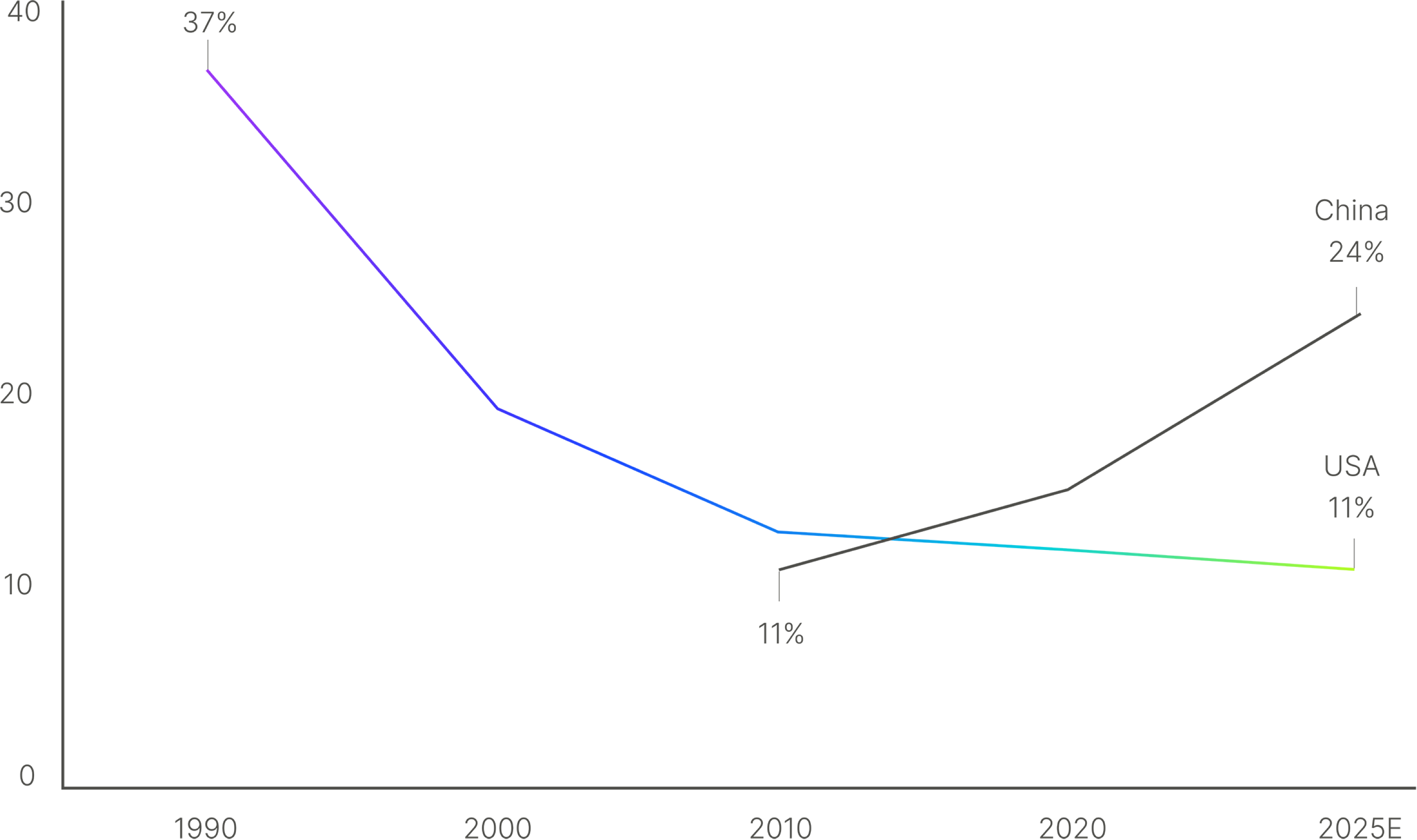 Percent of global semiconductor fabrication capacity for 300 mm wafers
With today's explosion in artificial intelligence and robotics, the number of chips needed year over year is increasing exponentially. However, the number of chips we can produce is bottlenecked by the number of semiconductor fabs we have. At the same time, we face the challenge of China's rapid semiconductor progress and its plans to win the AI race against the United States.
The rising costs to build and outfit advanced semiconductor fabs, coupled with critical gaps in our domestic supply chain, are preventing us from realizing the full potential of returning America to dominance in semiconductor production.
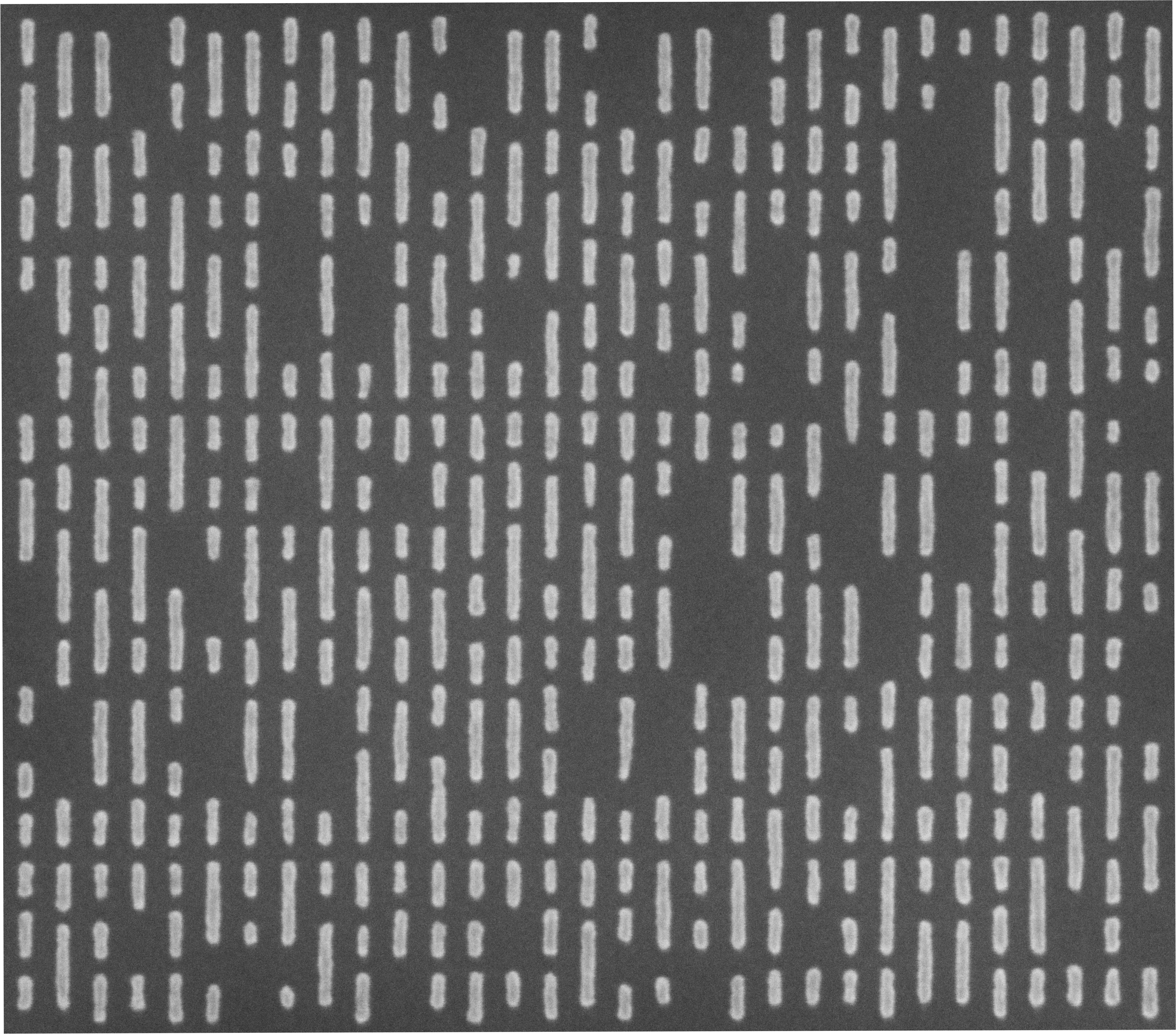 Random logic contact array of 12 nm critical dimensions and 13 nm tip-to-tip spacing printed with high pattern fidelity.
Substrate was founded to return the United States to dominance in semiconductor fabrication on three core beliefs:
- The cost of semiconductor fabrication is out of control, and it will only continue to trend upward without radical new technological innovation
- The United States is dangerously reliant on sources of geopolitical and supply chain risk that we do not directly control
- The only chance the United States has to return to dominance in semiconductor production would be to create a new type of more vertically-integrated foundry, one that continues pushing Moore's Law in both performance and cost
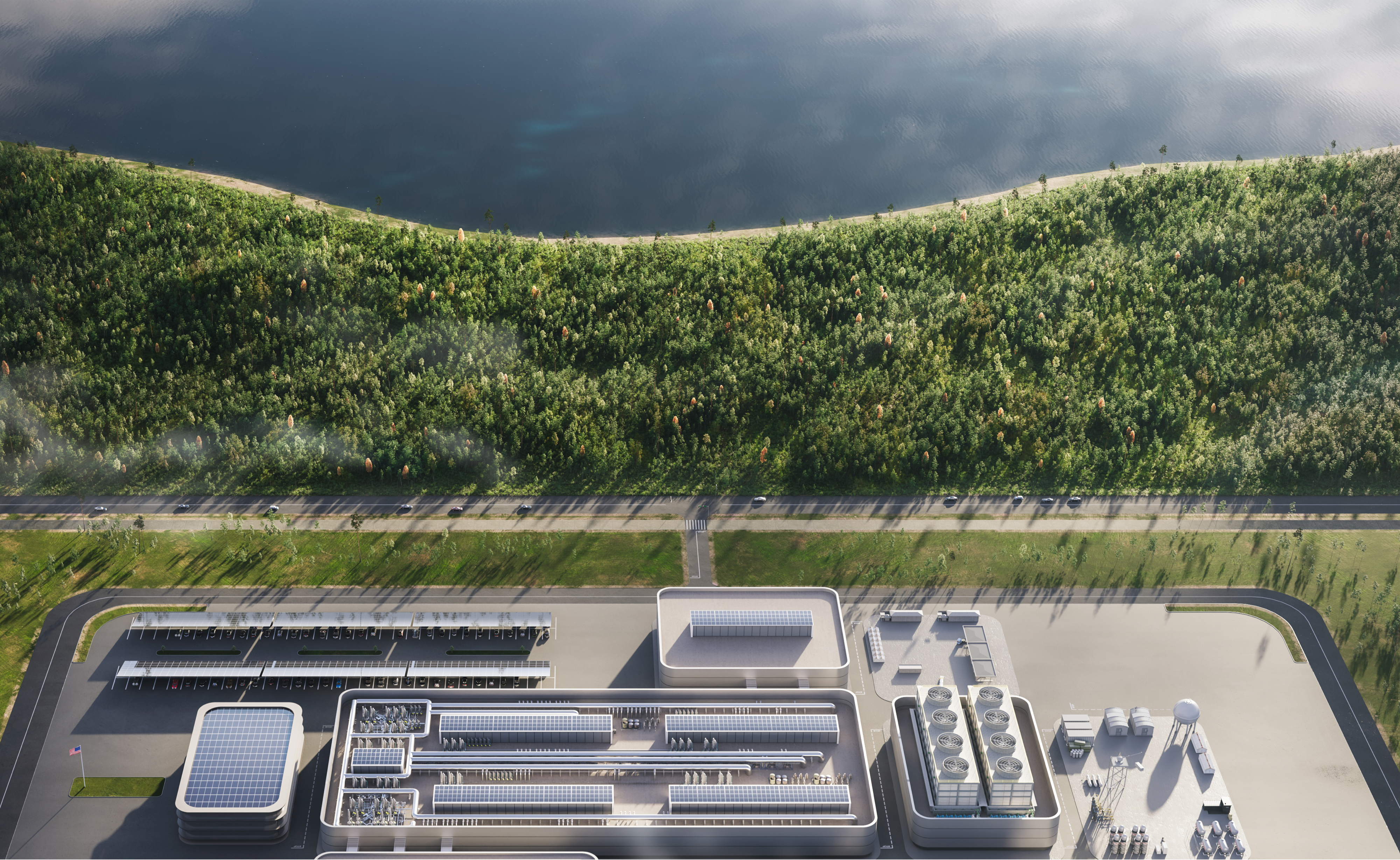
To achieve this, Substrate is building next-generation semiconductor fabs to return America to dominance in semiconductor production and will use our technology—a new form of advanced X-ray lithography—to power them.
Harnessing X-rays
Our results shown here can be compared with the current industry's "high numerical aperture" (High NA) EUV lithography and are equivalent in resolution to the 2 nm semiconductor node, with capabilities to push well beyond.
To accomplish this, we had to invent a new technology capable of producing the critical patterns required for today's advanced silicon, which was lower cost, less complex, more capable, and faster to build.
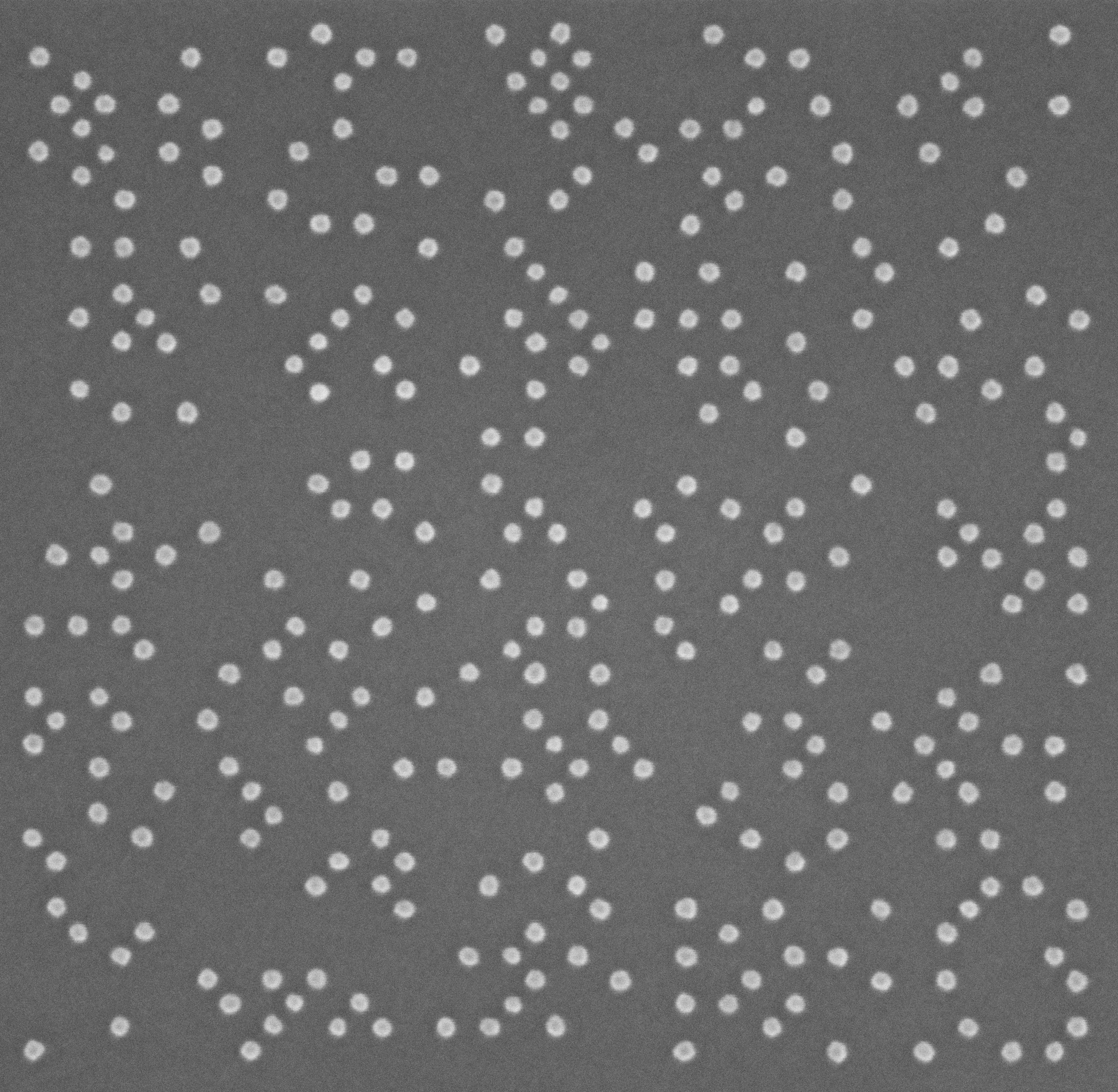 Random vias with 30 nm center-to-center pitch with superb pattern quality and critical dimension uniformity.
The team at Substrate has designed a new type of vertically integrated foundry that harnesses particle accelerators to produce the world's brightest beams, enabling a new method of advanced X-ray lithography. Our accelerators create and power beams that generate light billions of times brighter than the sun, directly into our lithography tools, each using a completely new optical and high-speed mechanical system to produce the smallest of features needed for advanced semiconductor chips.
While current approaches are reaching their limits, leading to increasing costs and complexity, all of our inventions are designed to work together to extend Moore's Law for years to come.
Our light source begins with radio-frequency cavities accelerating pulses of electrons using powerful electric fields. The electrons ride each successive wave, gaining energy and increasing their velocity to near the speed of light. To produce light, these charged, highly energetic electrons traverse a gauntlet of strong alternating magnetic fields, which force them to release their energy as bursts of brilliant, intense light. These bright pulses of light are transported and shaped by a succession of perfectly polished optics all the way to the silicon wafer.
Atoms and Angstroms
As with semiconductors and the eponymous Silicon Valley, the history of particle accelerators is deeply rooted in the San Francisco Bay Area. In the early 1930s, Ernest Lawrence at the University of California, Berkeley, constructed the first successful cyclotron—a compact device that used magnetic fields to accelerate protons. His invention launched a new field of physics and decades of scientific discovery.
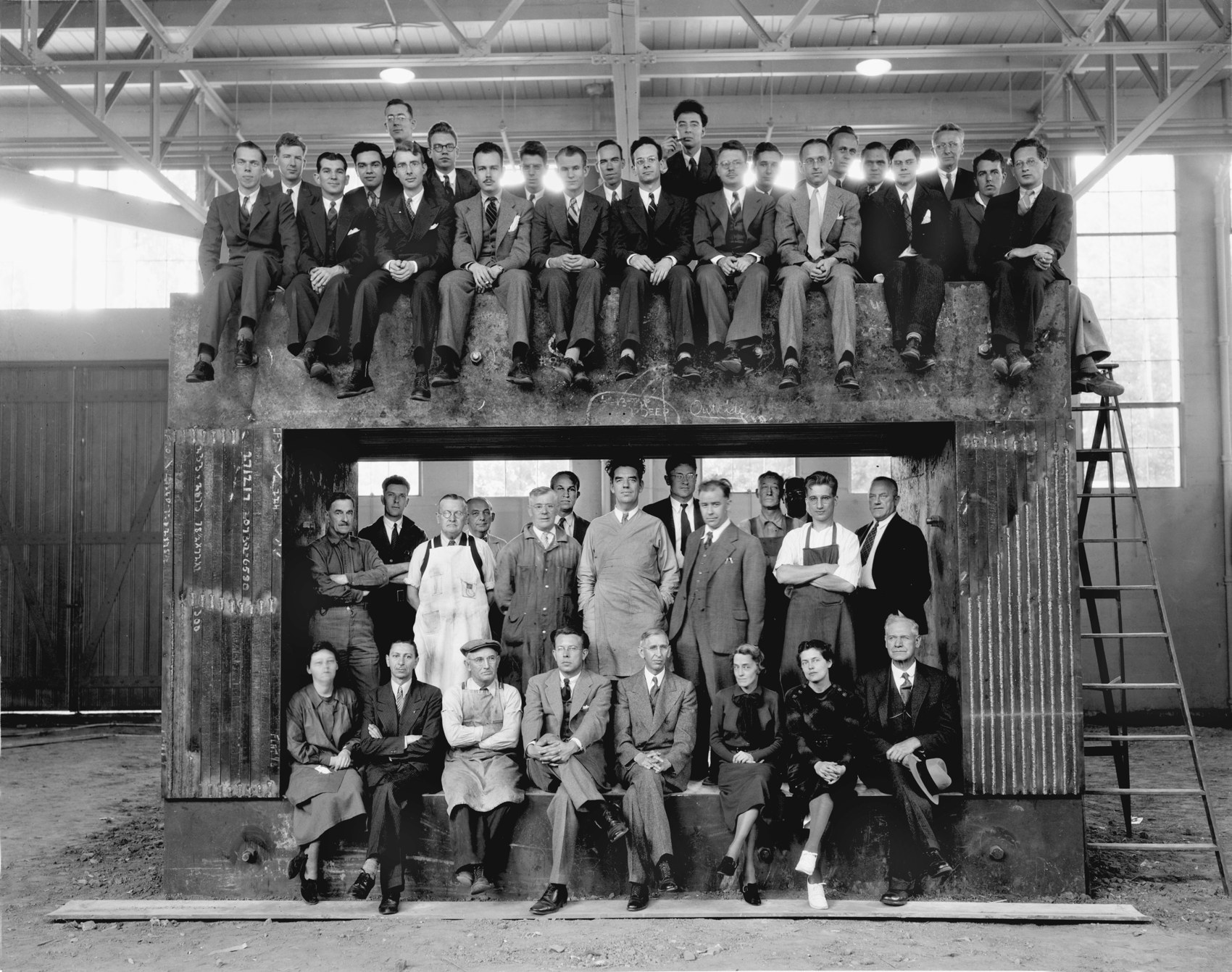 Ernest Lawrence and his team sit atop a giant magnet, a small part of the first cyclotron accelerator.
Courtesy of Lawrence Berkeley National Laboratory — Berkeley, August 1938
The laboratory he established became a cradle of accelerator innovation, producing increasingly powerful machines, such as the 184-inch cyclotron, that helped drive physics research during World War II. After the war, Lawrence's influence extended across the Bay with the founding of Lawrence Livermore National Laboratory and later SLAC National Accelerator Laboratory at Stanford, whose two-mile linear accelerator opened in 1966 as the longest in the world.
It is fitting that Lawrence's significant contributions to America's national security, which began with the Manhattan Project, live on today in the field of particle physics and, now, through advanced semiconductors.
These powerful accelerators have been used to illuminate the hidden structures of the universe and push the boundaries of fundamental science for many years now. By building on decades of progress at American National Labs and harnessing machine learning, Substrate can now design and operate these complex systems in high-volume manufacturing.
Using a particle accelerator to build the ultimate lithography machine presents new challenges, ones that have led us down a completely different pathway than others have explored before, and to results previously thought impossible.
American Lithography
The history of advanced lithography is one of American scientific ingenuity and commercial missteps.
EUV lithography research began in the '90s at the U.S. National Labs, where much of the early source, optics, and resist technology was developed. Despite these fundamental advances, American attempts to commercialize these technologies stalled after timelines and costs rose dramatically. This led to the key intellectual property and manufacturing leadership ultimately being transferred and licensed abroad, cementing today's foreign dominance and monopoly in lithography tools.
We deeply respect the achievements of the pioneers and companies who created today's AI semiconductor revolution, and the decades of incredible engineering that went into the creation of modern miracles like EUV. But for America to regain its rightful place as the leader in semiconductor production, we cannot repeat the same mistakes of the past.
Our team has designed, fabricated, and polished optics, formulated marvels of chemistry, machined and assembled tons of metal to produce a new type of advanced lithography built from the ground up for high-volume manufacturing—a feat of engineering no one thought possible for a startup.
Over the past several years, we have invested in building out our supply chain and continue to increase our vertical integration, enabling us to move at speeds usually unimaginable in the semiconductor industry. More recently, we completed our first in-house production-quality 300 mm wafer lithography tool, which operates at the extreme G-forces required to meet the throughput of a leading-edge fab.

A Billion Wafers Per Year
Developing the key technologies of the future—like advanced AI and robotics—depends on an exponential increase in advanced chips. Over the coming decades, the yearly demand for chips will not be measured in the tens of millions of wafers, but in the billions.
While many people are familiar with Moore's law, Rock's law is the second most important law in semiconductor fabrication. It observes that the cost of building a leading-edge semiconductor fab has roughly doubled every four years, with facilities rising from over $5 billion in the early 2010s to around $25 billion today.
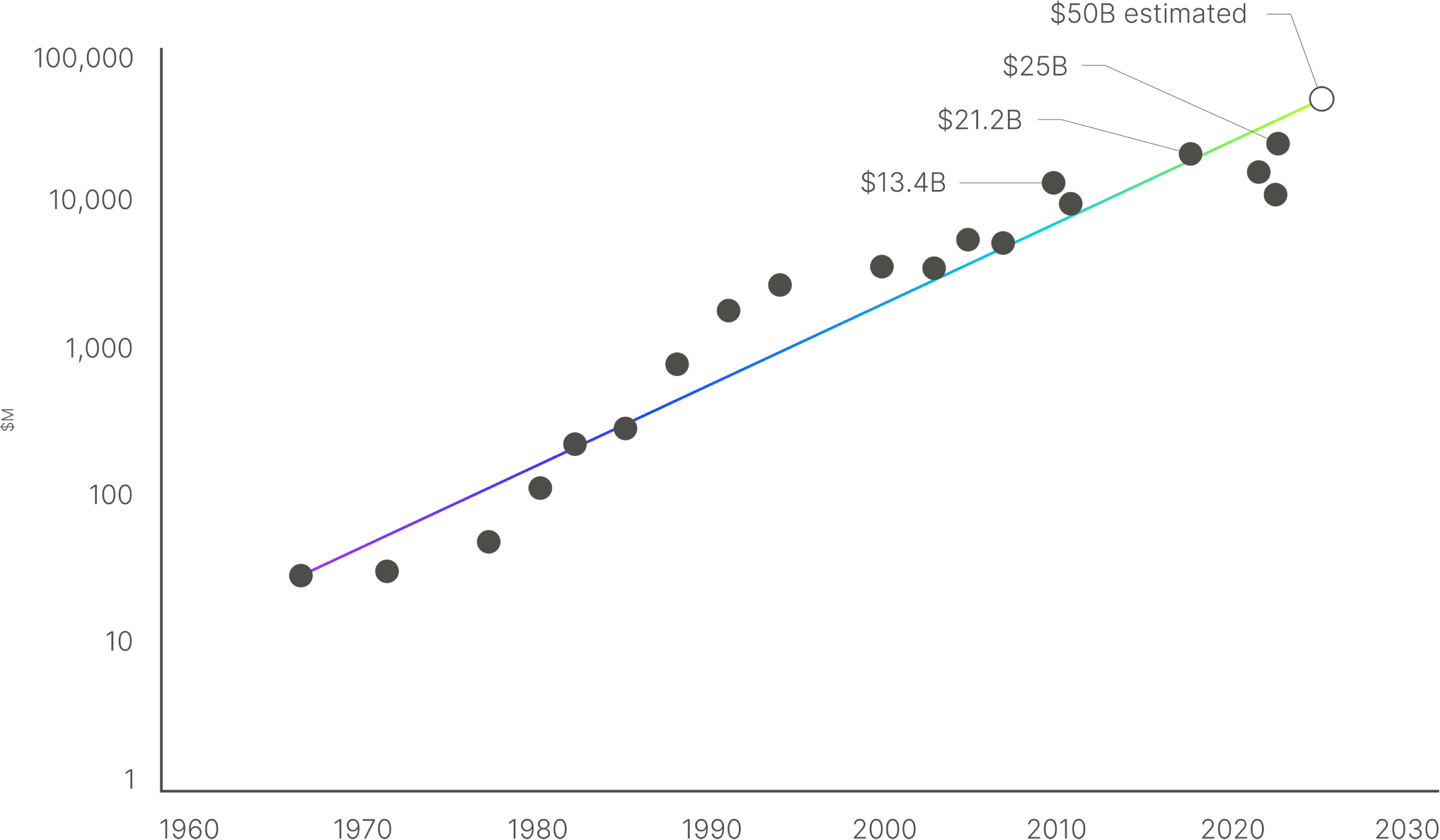 Leading-edge semiconductor fabrication facility cost over time which follows a steady upward trend
By 2030, wafers will cost $100,000 each, and fabs will cost over $50 billion each. In this future, only the largest companies will be able to afford to build products that leverage leading-edge silicon. The economics of this scaling are more daunting than the physics. This economic model feels broken.
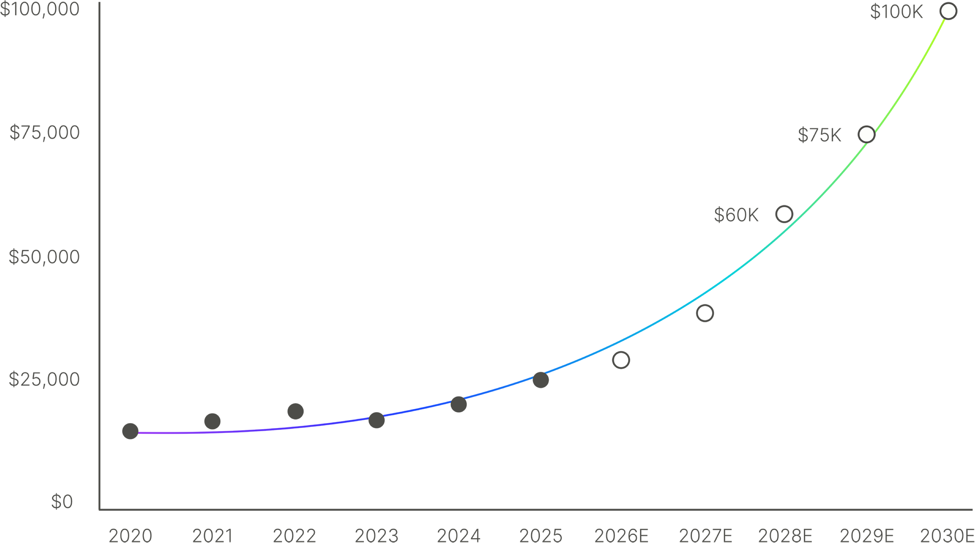 Historical and expected costs of a leading-edge wafer to end customers
At Substrate, we have a pathway to reduce the cost of leading-edge silicon by an order of magnitude compared to the current cost-scaling path we are on. By the end of the decade, Substrate will produce wafers closer to $10,000, not $100,000.
To achieve a world where the proliferation of advanced chips matches the scientific future we want to imagine, we need to lower the cost of silicon wafers while expanding the number of companies and innovators who can design and build leading-edge chips.
Computer-generated chips
Designing chips is expensive and complex. For the most challenging designs, few companies can manage the complexity, and even fewer can afford the cost.
AI models already assist chip designers in creating custom silicon, and in the near future, they will surpass humans at this task. The cost of design and verification will plummet to near-zero, and designing complex silicon will become something almost any company can afford.
Once this happens, the bottleneck will become the fabrication and manufacturing of these chips.
Substrate understands the power of AI in accelerating innovation in manufacturing. From day one, we have leveraged GPUs and TPUs to accelerate solving problems previously thought to be intractable. By building end-to-end simulations of the physics governing our machines, the transistors we will create, and the final designs they will power, we have compressed problems that would have previously taken years to solve into days.
America's technology industry is already building the largest AI factories in the world. Substrate will build the world's most advanced AI-designed semiconductor foundries to supply America's AI industry into the coming decades and ensure that our future powerful AI systems run on an American stack, top-to-bottom.
Who will control the future?
For decades, we have repeatedly underestimated China's ability to innovate while simultaneously underinvesting in our own. Substrate believes that by the end of the decade, China will have achieved self-sufficiency in most, if not all, of the semiconductor wafer fabrication tools required to have a wholly domestic semiconductor fabrication industry, including advanced lithography.
The semiconductor industry stands at a crossroads. China has made advanced semiconductor production a national priority, investing unfathomable sums into domestic tooling and manufacturing advances. We may soon witness a similar tectonic shift in semiconductor production where technological capabilities and leadership ability abruptly change, leaving us as a country scrambling to respond to capabilities we never anticipated emerging so rapidly.
By the end of this decade, either America or China will control the future of computing and the AI industries built on top of it.
Failure is not an option, we must try
For years, many have spoken of the need for a new pure-play American foundry, yet view it as an impossible task. History repeatedly shows that American science and engineering solve impossible tasks. As we rush to build more current-generation semiconductor fabs in America today, we need to start immediate work on building the semiconductor fabs of tomorrow.
The stakes are too high for the United States not to try everything we can to solve both one of our most significant technological gaps and our biggest opportunities to reclaim leadership over the technologies we pioneered. If China surpasses the United States in advanced semiconductor production, it would fundamentally shift global technological and economic power, giving China dominant leverage over critical supply chains that power everything from AI to military equipment.
We stand on the shoulders of the American giants who built this industry. Shockley. Moore. Noyce. Grove. Chang. Huang. We want you to join us in making the next century and future of Moore's Law an American one.